Gas sensors are an essential component for a broad range of applications, for example in the medical and diagnostic fields, indoor and outdoor air quality monitoring systems, environmental studies, and the automotive industry. They are gaining importance as the desire for rapid detection of toxic or organic gases is growing among the population.
There are different types of gas sensors available. Most of the commercially available gas sensors suffer from high power consumption and high operation temperatures. They are often bulky and not suitable for integration into mobile or wearable devices. Among various sensing techniques, optical gas sensors can offer higher sensitivity, long-term operation stability and much shorter response times, making them suitable for real-time and in situ detection.
Most of the optical gas sensors rely on absorption spectroscopy, where a gas is detected by measuring the light absorption (due to the interaction of light with that gas) as a function of the wavelength. Many important organic and inorganic molecules such as CO2 have characteristic absorption lines in the infrared region.
Optical gas sensors can be integrated on a chip using photonic integrated circuits (PICs). PICs tailored for applications such as sensing, spectroscopy, diagnostics, biomedical imaging, and telecommunication rely on infrared (IR) photodetectors (PDs) that are coupled to waveguides. Photodetectors for the near-IR wavelengths are mainly based on Si and Ge. Mid-IR PDs, however, are typically made from exotic compound semiconductors such as InGaAs and HgCdTe with the downside of higher manufacturing cost and harsh operating conditions. A key requirement for broad applicability of PICs is the integrability of IR PDs on photonic waveguides. This is not fulfilled for the conventional Mid-IR materials because their (epitaxial) growth requires high temperatures which are not compatible with PIC thermal budgets. This creates a high demand for IR PDs with high manufacturability at low-temperature budgets.
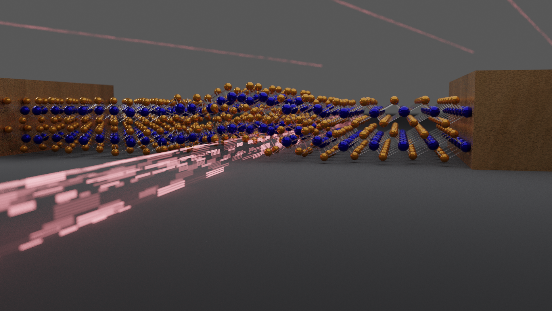
" Schematic image of a layered PtSe2 photodetector integrated on a photonic waveguide"
Two-dimensional (2D) materials have attracted tremendous attention in the optoelectronic field due to their unique characteristics such as broadband optical absorption, high carrier mobility, mechanical flexibility, and ease of integration.
Platinum diselenide (PtSe2) is a transition metal dichalcogenide (TMD) which behaves as a semiconductor with an indirect bandgap of 1.2 eV as a monolayer and as a multilayer material, becomes semi-metallic with zero bandgap.
A major advantage of PtSe2 is the possibility of direct, large-scale growth on various substrates at temperatures below 450 °C using the thermally assisted conversion (TAC) technique. In combination with the potential for selective and conformal deposition PtSe2 is suitable for back-end-of line (BEOL) integration on electronic and photonic wafers.
In this work, we demonstrate the use of layered platinum diselenide (PtSe2) as an integrated infrared photodetector on Si photonic waveguides for the wavelength 1550 nm with high responsivity.
We have fabricated waveguide integrated PtSe2 detectors using direct growth and conventional wet transfer, and we have studied the device performance and material quality of both approaches through analytical, electrical, and optical characterization.
A responsivity of 11 mA/W was achieved for a directly grown PtSe2 photodetector, with a fast response time of 8.4 μs which is limited by our measurement setup. Our Fourier-transform infrared (FTIR) measurements indicate that PtSe2 is also suitable for photodetection in the mid-IR regime up to 30 µm wavelength, which makes it a perfect material for gas sensing and imaging.
Our results show that multilayered PtSe2 is a promising candidate for high-responsivity optoelectronic applications in commercial semiconductor technology platforms. This also includes silicon nitride (SiN) or other photonic platforms, as the direct TAC growth does not require any crystalline surfaces, in contrast to epitaxial processes. In summary, this work highlights the potential of PtSe2 for wafer-scale integration of waveguide coupled photodetectors.

Shayan Parhizkar, lead author of the paper and ULISSES researcher with AMO GmbH
Full reference:
- « Two-Dimensional Platinum Diselenide Waveguide-Integrated Infrared Photodetectors », Shayan Parhizkar, Maximilian Prechtl, Anna Lena Giesecke, Stephan Suckow, Sophia Wahl, Sebastian Lukas, Oliver Hartwig, Nour Negm, Arne Quellmalz, Kristinn Gylfason, Daniel Schall, Matthias Wuttig, Georg S. Duesberg, and Max C. Lemme, ACS Photonics
- DOI: 10.1021/acsphotonics.1c01517
 This project has received funding from the European Union’s Horizon 2020 research and innovation programme under grant agreement No 825272 (ULISSES).